Data size and functionality requirements for computing are increasing, according to the expectation that hardware performance will continue to improve, irrespective of the actual implementation. However, the end of roadmapped technological scaling is anticipated in a few technology nodes, mainly for cost reasons down to the 7nm FinFET gate length node.

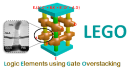
In this context, vertical integration is an attractive approach thanks of its intrinsic 3D nature, which is more favorable to scale the contacted gate pitch. The vertical NW (nanowire) array based transistor is much easier to manufacture because the gate length is simply defined by the thickness of the deposited gate material. A few years ago, the industry considered this transistor to be too extreme a device modification. However, very recently, this situation has changed, with several major actors (Intel, TSMC, IMEC) that now consider the concept of vertical NW transistors as a credible option for sub-7nm node. Further, enhanced functionality can be achieved with doping techniques leading to the stacking of N and P type transistors. Accordingly, new architectures are mandatory. Many conceptual ideas already exist for non-conventional logic circuit design. They are usually based on emerging device technologies which have been developed and extensively characterized at laboratory level. However, due to the broad gap between device research and technology optimization, no vertical logic circuit demonstrators exist. The LEGO project is intended to fill the gap between device research and innovative logic circuit implementation through the following objectives:
- demonstrate the proof of concept of stacked vertical NWFET for non-conventional logic circuit
- develop a design kit including compact models to support the circuit design flow
- prove enhanced logic functionality and logic circuit operation in terms of propagation delay, dynamic and static power consumption, resilience to temperature and supply voltage variation
- assess the technology roadmap improvements and the associated logic performance metrics.

The partners of the highly qualified and motivated LEGO consortium are especially relevant to address this disruptive design-technology co-optimization: three academic laboratories (LAAS, IMS, INL) bringing appropriate contributions based on excellent expertise and high-level research in the fields of NW fabrication, electrical characterization, compact modelling, and innovative circuit design. The unique technological skills, with five patents held by LAAS on the scaled vertical NW transistor process technology, offer a great opportunity for success in this very high gain project. Previous work, initial developments and past collaborations mean that there are no showstoppers and that the consortium is confident that the project will succeed. The main risks are therefore the delay in technology fabrication. This will be mitigated by the use of initial technology, which enable exploration of novel circuit designs without searching for optimal parameter values. Two logic styles that are well suited to regular fabrics of vertical NWFETs using in LAAS technology:
- majority inverter graphs (MIG) using multiple electrode NWFETs
- pass-transistor logic (PTL) using uniform and hybrid n/p NWFETs

Huge gains in silicon area are expected through the combination of extremely small elementary device footprint and minimal device usage with MIG and PTL design styles. For example, a 1-bit full-adder can be built in PTL with just 3 vertical hybrid n/p nanowires instead of 31 nanowires in standard logic. Such 10x reductions in complexity will lead to similar gains in energy consumption and delay. Therefore, the LEGO project specific objectives are:
- Ground-breaking stacked vertical n- and p- NW Field Effect transistor
- 3D innovative elementary logic building blocks based on stacked n- and p- NW FET
- 4-bit ALU using the actual implementation of two logic styles based on stacked vertical NWFETs.
